
A microwave oven is the key to 2-nanometer chip manufacturing
|
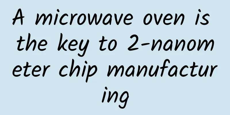
A home microwave oven modified by scientists is helping to create the next generation of cell phones, computers and other electronics, an invention that has proven to overcome a major challenge facing the semiconductor industry. The relevant research results were published in the scientific journal Applied Physics Letters under the title “Efficient and stable activation by microwave annealing of nanosheet silicon doped with phosphorus above its solubility limit”. James Hwang, professor of materials science and engineering at Cornell University, is one of the corresponding authors of the paper. (Source: Applied Physics Letters) As chips get smaller, silicon must be doped, or mixed, with higher concentrations of phosphorus to generate the required electrical current. Today, semiconductor manufacturers are reaching a limit where conventional methods of heating highly doped materials are no longer sufficient to produce stable semiconductors. Semiconductor maker TSMC thought microwaves could theoretically be used to activate excess dopants. But, just as a household microwave oven sometimes heats food unevenly, previous microwave annealing setups tended to create “standing waves” that prevented uniform activation of the dopants. Figure | Chip under an electron microscope (Source: Wikipedia) To this end, TSMC worked with Hwang to selectively control where the standing waves occur through a modified microwave oven, thereby activating the dopants just right without overheating or damaging the silicon crystal. "This discovery could be used to manufacture semiconductor materials and electronic products that will be produced around 2025," Hwang said. Even more, Hwang said: "Currently, only a few companies are producing 3-nanometer semiconductor materials. This new microwave method has the potential to enable chipmakers such as TSMC and Samsung to shrink the size to 2 nanometers." Photo: James Hwang (right) next to the modified microwave oven. It is reported that this breakthrough may change the geometry of transistors used in chips. For more than 20 years, in order to fit more transistors on each chip, transistors have been made to stand upright like dorsal fins. In recent years, chipmakers have begun experimenting with a new structure in which transistors can be stacked horizontally. Microwave annealing, which makes more doped materials possible, is key to making the new structure possible. References: https://aip.scitation.org/doi/10.1063/5.0099083 |
>>: It’s true that your brain stops working! Thinking can also make you tired!


Recommend
The Cocos Developer Platform White Paper will be officially released on October 28
[[121407]] <span lang="EN-US" style="font-size...
How long can a battery smaller than a grain of salt provide power?
Batteries are an essential part of our lives. The...
99% of startups fail: Is decentralization the cure?
A few days ago, I wrote an article titled " ...
Lei Jun's three-hour talk: I don't have time to worry
[[134230]] Every once in a while, this star entre...
Great! Scientists have invented a new fabric that automatically cools you down when you wear it
Summer has arrived as promised. Every corner of t...
Will your ID card and mobile phone be demagnetized if placed together? How many of these 7 common problems in life do you know?
Will my ID card be demagnetized if I put it behin...
Toutiao Information Flow Luban Introductory Course [Basic Concepts] Tutorial
Chapter 1: Basic Concepts 1.1: What is informatio...
5,000 words of in-depth information to reveal the secrets of offline event promotion!
When it comes to organizing events, it is a love-...
Why did the American version of Wang Sicong reject the 10 billion yuan fortune and become obsessed with Japanese culture?
For many viewers, the "enlightenment" o...
360 has little chance of success in returning to its old business of mobile phones
According to media reports, Qihoo 360 has announc...
How to do To B content marketing?
What are the similarities and differences from C ...
Don’t know where to start with CPC optimization? This is how Ready Player One plays!
“ Information flow ”, “oCPC”, and “creativity”, w...
Make money without goods on Taobao#《How to make money with Taobao virtual projects without copyright risk》
My old fans all know that I seldom give public tr...
Why do some girls have more body hair than boys? Be careful of this disease!
Every summer, some girls will face a different pr...
Why is there no winner in long-term gambling? You need to understand the "Gambler Loses All Principle"
Why not gamble? This question needs to be discuss...